ESP32 Digital Guitar Effects Pedal
A digital multi-effects guitar pedal taken through three generations: an FPGA prototype, a custom ESP32 PCB, and a low-noise redesign currently in progress. Documented on my LinkedIn.
Summary
A digital guitar effects pedal I'm designing and building from scratch, now on its third version. v1 (FPGA): My first pedal ran the audio processing in hardware on an FPGA. It taught me real-time audio fundamentals and audio codec bring-up. v2 (ESP32 dev board): I moved to the ESP32-A1S and its ES8388 codec for a more flexible, firmware-driven multi-effects platform. I validated the full audio path on a dev board with a clean passthrough first, then added reverb, bit crusher, tube screamer, and overdrive. v3 (custom PCB, in progress): My own 4-layer circuit board built around the ESP32-A1S. I scrapped my first layout before fabrication, and the current design is about 50% smaller and 50% cheaper. It adds USB-C with auto boot/reset, microSD effect loading, a 0.96" OLED, and a push rotary encoder, along with a low-noise power architecture and a deliberately gain-staged analog front end.
Problem / Goal
Build the best-sounding multi-effects pedal I could for the cost, on my own hardware and firmware. Digital pedals often suffer from power supply noise, poor gain staging, and early clipping. The goal was to solve these at the architecture level instead of patching them later.
What Was Built
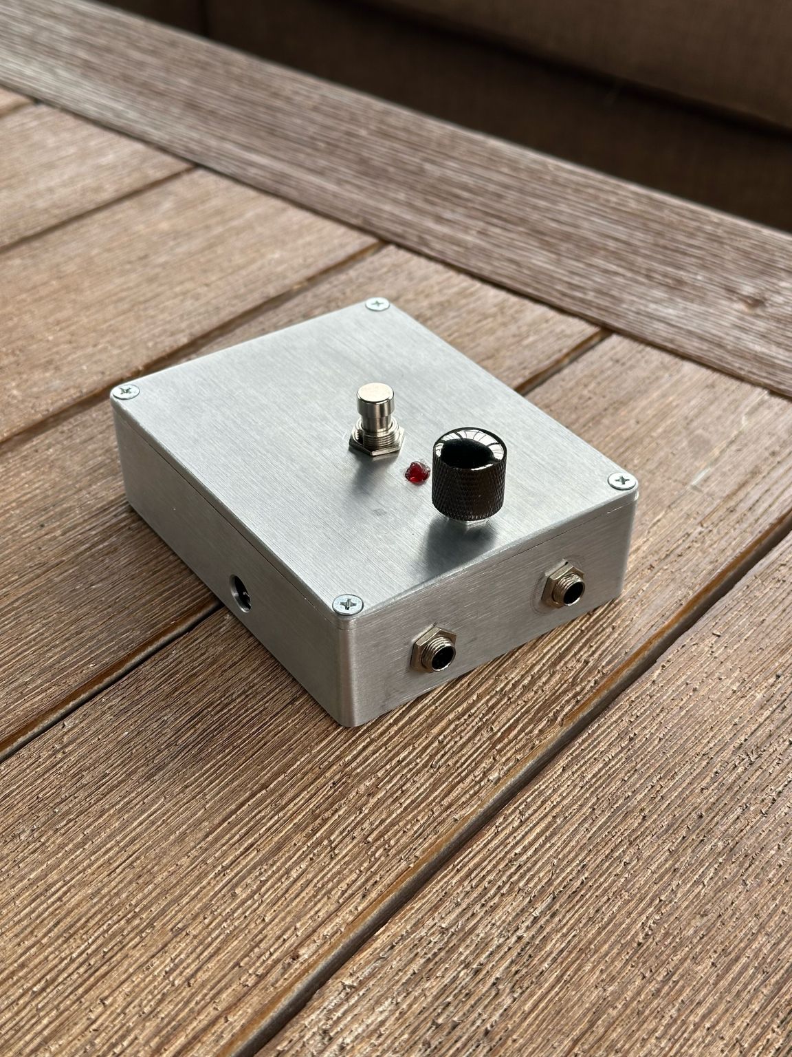
v2 (ESP32 dev board): - Clean audio passthrough validated end to end - ESP-ADF firmware running four real-time effects: reverb, bit crusher, tube screamer, and overdrive - Multiple effects, built in combination with AI for faster development, which include reverb, distortion, tube screamer, and a bit crushe v3 (custom PCB, in progress): - 4-layer KiCad PCB with dedicated GND and power planes and an ENIG finish, partly assembled by JLCPCB, with the ESP32-A1S, encoder, and buck converter hand-soldered - CP2102N USB-C flashing with an auto-reset circuit for one-click programming - MicroSD effect loading, I2C OLED display, and push rotary encoder - Diode-OR USB and 9V power with P-FET reverse-polarity protection - Forced-PWM buck converter for the 3.3V digital rail, LT3042 low-noise LDO for a 5V analog rail - Unity-gain input buffer followed by a 0.68x divider so the ADC clips before the op-amp, with film capacitors only in the signal path - Finished 1590BB aluminum enclosure, ready for the board
Tools / Stack
Challenges
- Moving from FPGA to ESP32: I gave up hardware-level timing in exchange for much faster effect development - Cold solder joints and improper soldering technique. - Muddy, noisy audio in early ESP32 builds, traced to the ES8388 input channel configuration in ESP-ADF and to solder joint quality - Getting the ESP-ADF toolchain working on Windows took extensive debugging before I had a clean passthrough - The codec's analog supply is inside the A1S module and can't be filtered separately. I'm mitigating this with pi filtering and a forced-PWM buck that switches at 2MHz or higher, to avoid whine at light loads - The ES8388 programmable-gain amplifier has no attenuation, so the input divider had to be designed rather than assumed
What Was Learned
- Noise has to be designed at the system level from the start. Power supply choices matter more than firmware fixes. - Trust the datasheet over memory or rules of thumb. - Write decisions and non-goals down on purpose instead of letting them happen by default. - Validate the whole signal path with a simple passthrough before adding features. - Cutting scope is often the right engineering call. - Practical PCB skills: 4-layer stackups, DRC discipline, mixed JLCPCB and hand assembly, and reflowing castellated modules.